Every revision of the Havaxer 01, what changed, and what was measured on it.
The measurements are grouped by the feature they belong to. Each one is explained on the Features page; here are only the numbers, per version, because a measurement belongs to the board that produced it.
Version 1.0
| Design finished | 2026-07-05 |
| Put into production | 2026-07-06 |
| Inspecting | 2026-07-22 |
| Released | 2026-07-26 |
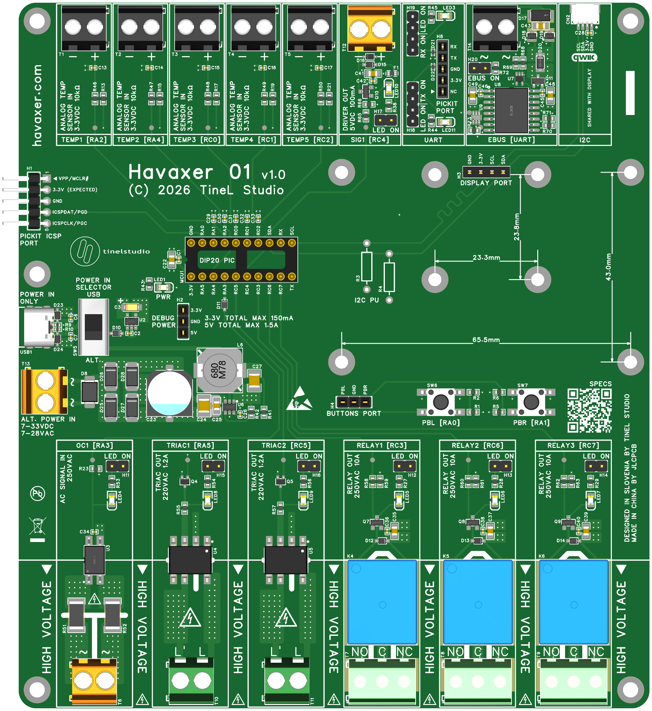
In PCB layout PDFopen_in_new you can find a complete and very transparent layout of the PCB, which, when printed on a paper, gets you a precise size and dimensions, too.
Next is a rendered 2D PCB with all components. Note that colors might not be correct.
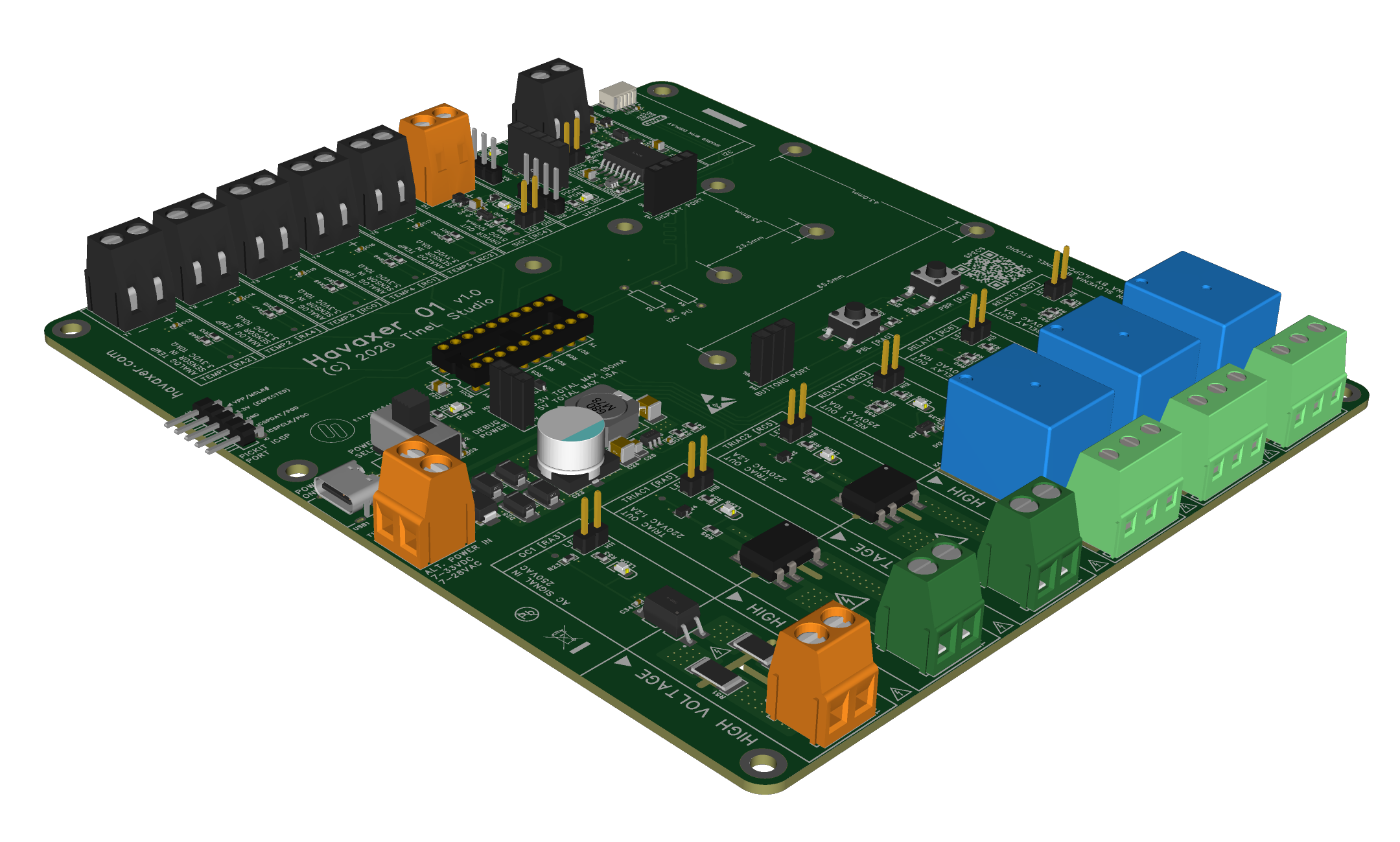
Next is a rendered 3D PCB with all components. Note that colors might not be correct.
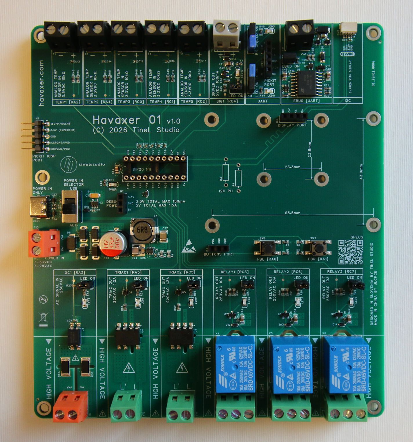
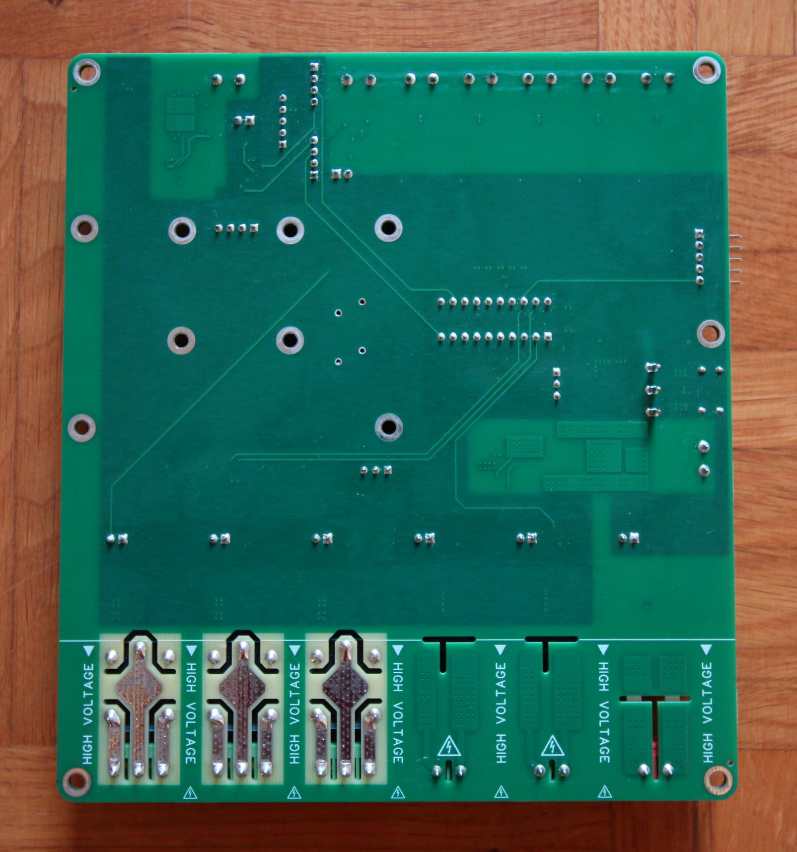
Next are some profile photos of the assembled board:
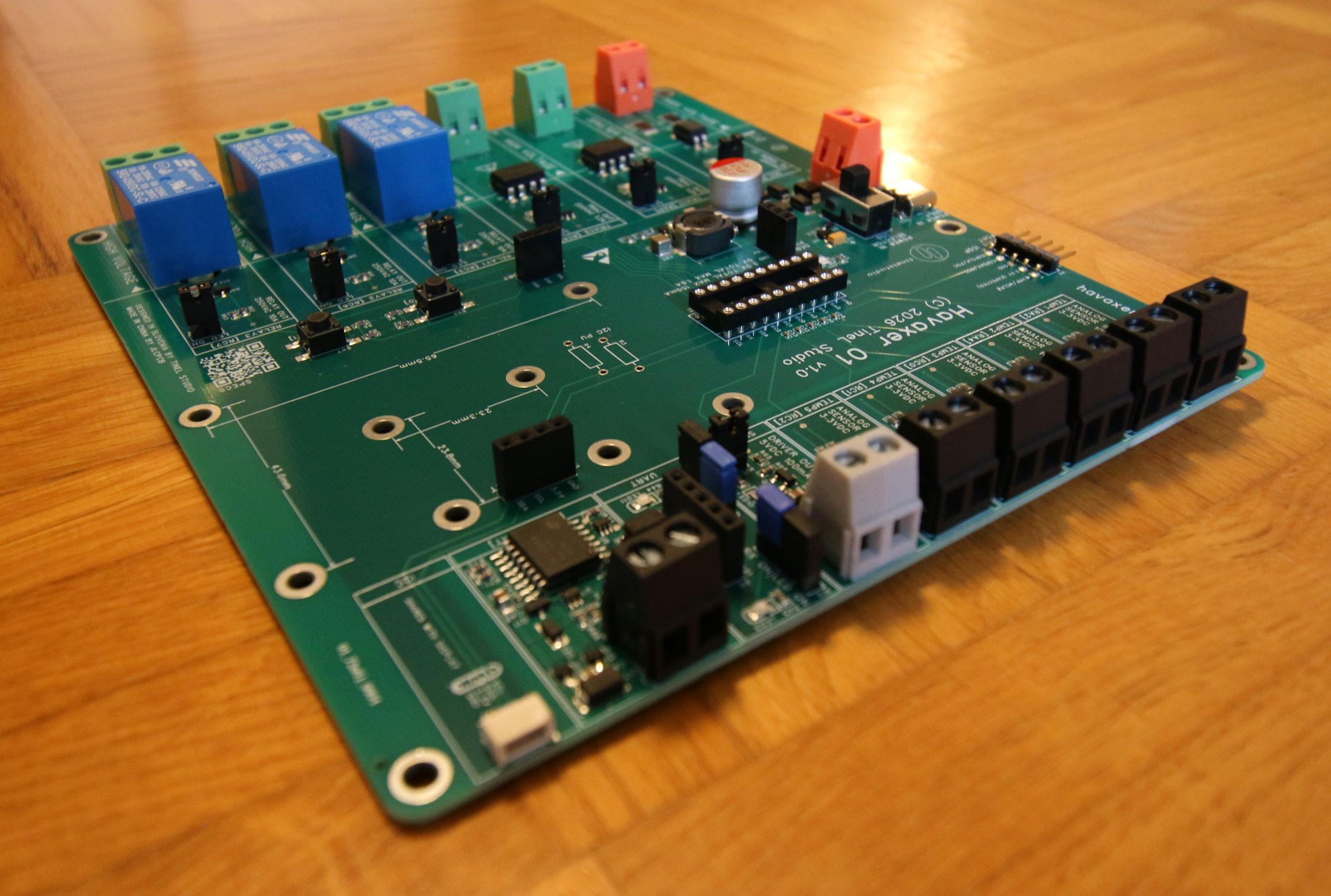
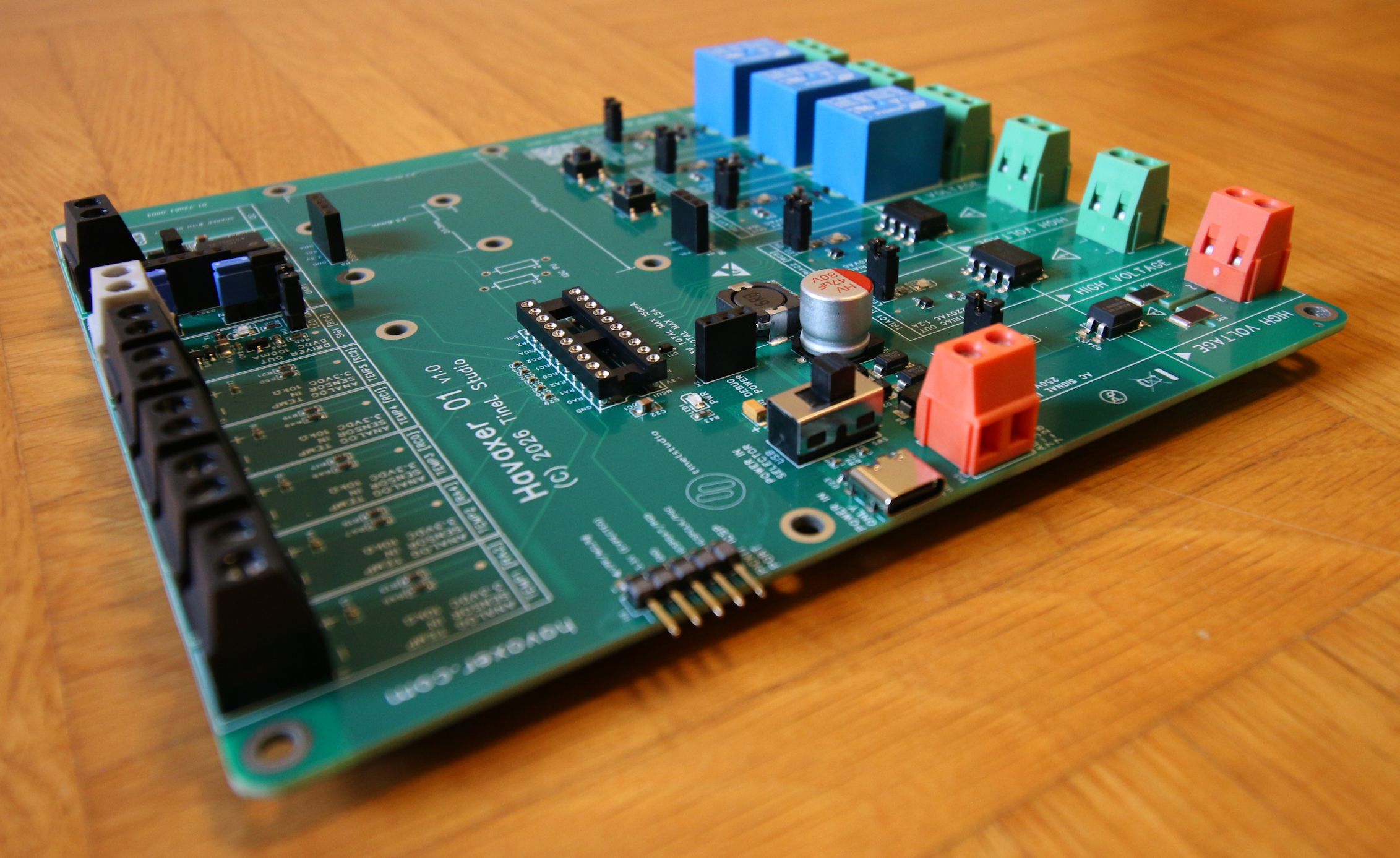
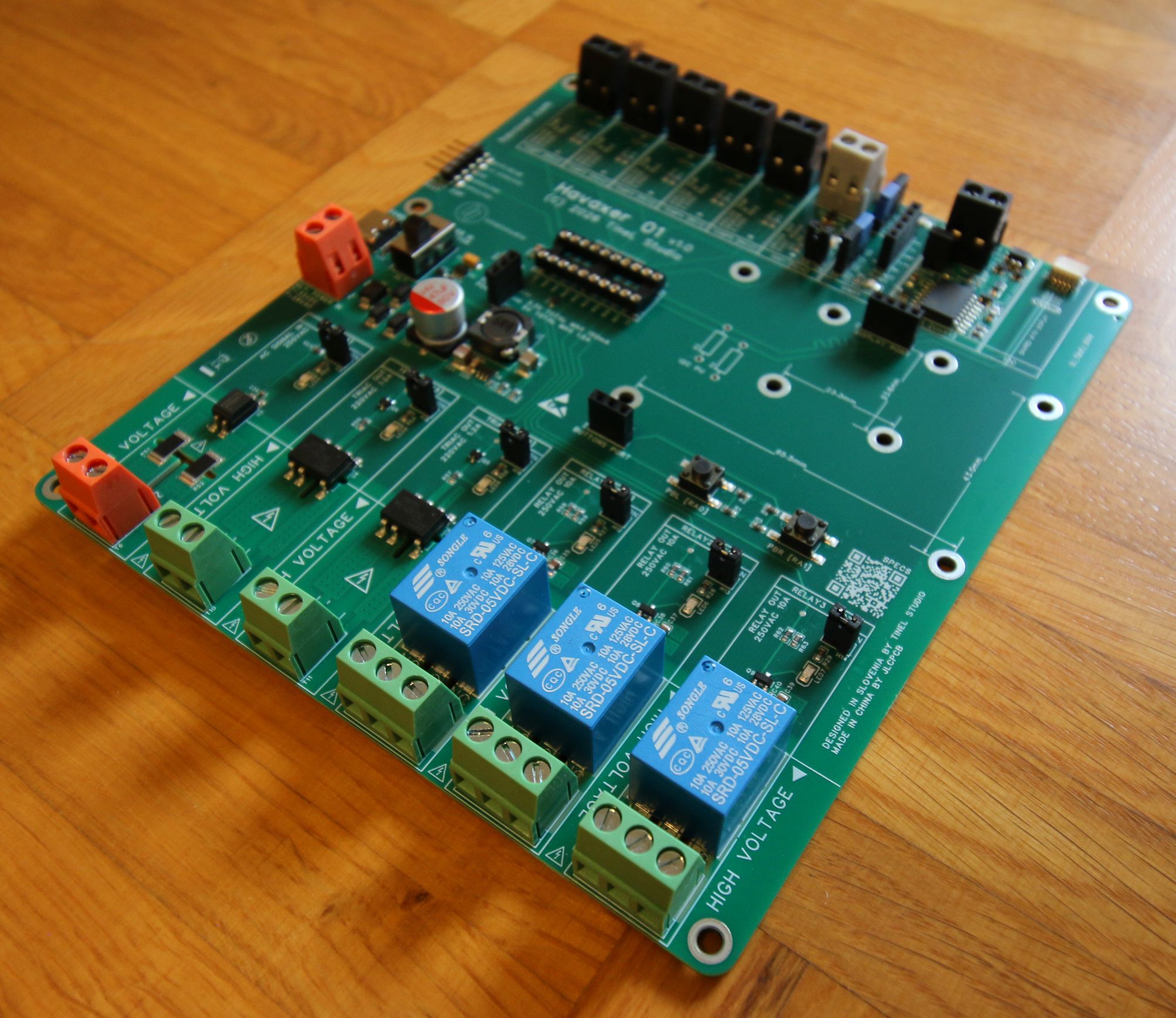
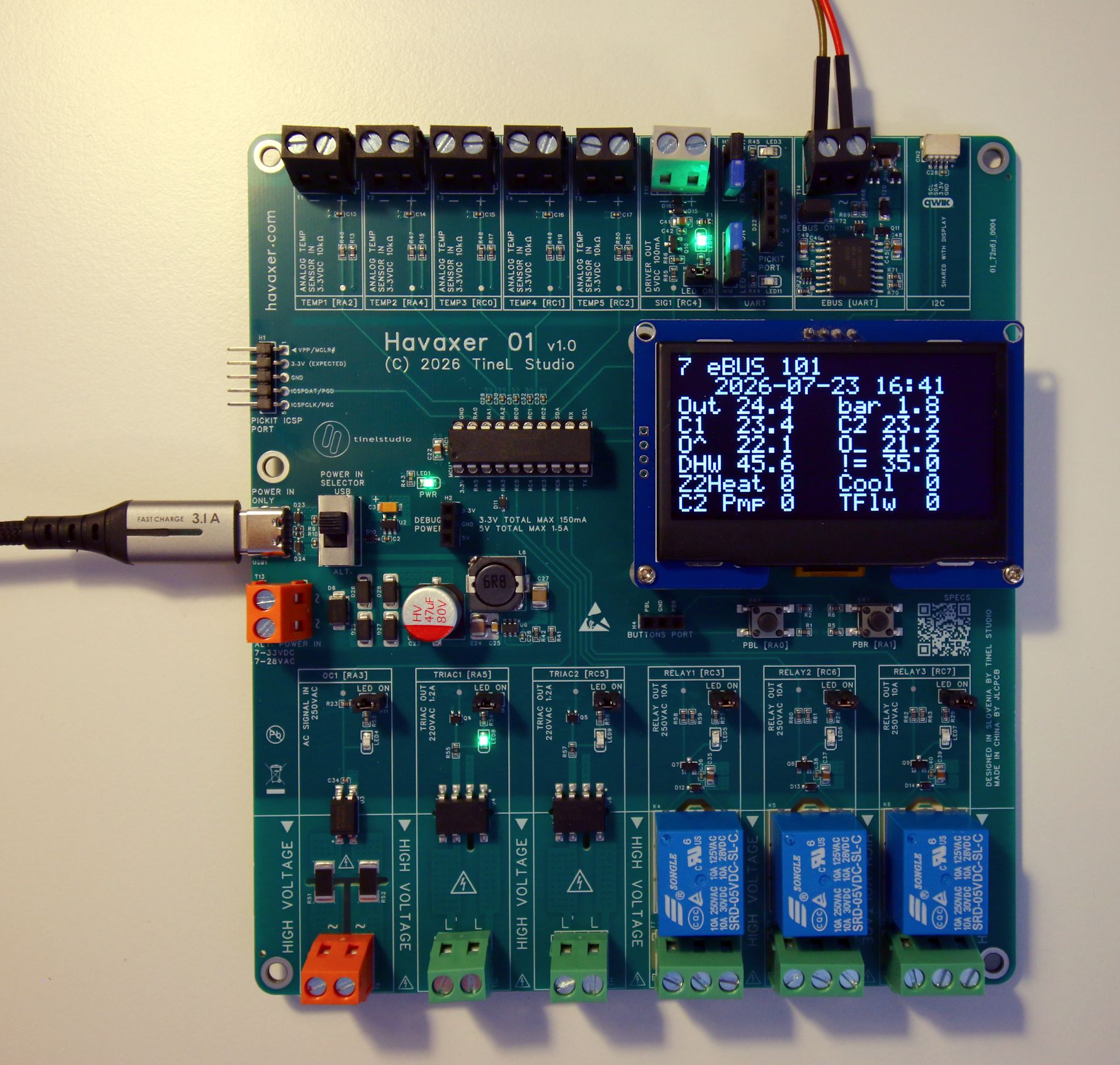
And a photo in action with a fitted optional 2.42" OLED, attached optional PIC18F16Q40 and connected optional USB A-C cable:
Known problems 1.0
-
Using the UART port standalone (no eBUS) has a known limitation. The RX line is known to leak a tiny amount of current - enough to cause signal noise. To prevent this, simply wire the right pin of the
EBUS ONheader (H20) to the board's ground.
Issue #25open_in_new -
The alternative power supply's printed range
7-33VDC / 7-28VACis over-declared at the AC end. Should read7-33VDC / 7-22VAC. On AC it is the peak that counts, and a 22 V RMS supply already peaks at 31 V.
Issue #26open_in_new
What changed since 0.9.5
Most changes are registered on GitHubopen_in_new.
The bridge rectifier became four discrete schottky diodes. The 0.9.5 board used a single 2 A bridge chip, and it was the weak point of the whole supply - at 6.64 V in and 600 mA out it reached 88 °C and the 5 V rail sagged to 4.84 V. The 1.0 board uses four SS34 diodes rated 3 A and reaches 53 °C at 7 V in and 970 mA out, with the rail holding 5.01 V. That is the single largest improvement between the two revisions.
The polarity inversion of transmit and receive linesopen_in_new of the eBUS adapter. It was done by inserting inverter gates between the adapter and the MCU, which also adds a degree of isolation.
Measurements 1.0
Test equipment: KWS-MX23 USBopen_in_new and KAIWEETS KM100sopen_in_new multimeters, power over USB at 5.06 V. Thermal images with an InfiRay P2 Proopen_in_new.
Analog temperature sensor input
Draw at rest is below the resolution of the test setup.
Mains signal input
- Draw from the board's 5 V rail: 0 mA, against 0.3 mA designed.
- At ~230 VAC the limiting resistors reach 38 °C (+14 K). Applied 240 VAC.
- Voltage across the optocoupler input: 1.1 VAC, matching the datasheet typical.
- Turn-on threshold, measured on DC: the firmware saw
OC1go active at 34.2 V and drop out again at 28.2 V. The 6 V of hysteresis is the PIC input's own Schmitt trigger, not firmware. - The indicator LED became faintly visible at 35 V and was clearly lit by 40 V - just above the point at which the input already reads.
Mechanical relay output
- Coil current at 100 % PWM duty, cold: 70.5 mA, against 80 mA designed.
- Coil resistance 70.0 Ω cold and 76.6 Ω warm, specified 69.4 Ω ±10 Ω.
- Drop across the driving MOSFET at 100 % duty: 114 mV, with 4.98 V in.
- ~230 VAC at 11.2 A for several minutes - deliberately above the 10 A rating - brought the relay area to 62 °C (+38 K). The relay body itself did not heat at all; the power traces underneath it did.
Relay coil PWM hold
| 100 % duty | 40 % duty | |
|---|---|---|
| Coil current, cold | 70.5 mA | 10 mA |
| Drop across the coil | 4.86 V | 1545 mV |
| Drop across the MOSFET | 114 mV | 3491 mV |
Roughly 60 mA saved per energised relay, which on a three-relay board is most of its total consumption.
Solid state relay output
- Drive current from the 5 V rail per triac: 8.5 mA, against 9.8 mA designed.
- Drive chain at 5.03 V in: 1135 mV across the triac IC - against 1.18 V typical in the datasheet - 3848 mV across the series resistor, 52 mV across the driving transistor.
- ~230 VAC at 1.35 A for several minutes, above the 1.2 A rating: 70 °C (+46 K).
Signal driver output
- At rest: 0 mA.
- Shorted, the current does not settle on one figure. It starts at roughly 160 mA and falls to about 120 mA over a minute as the PPTC fuse heats and its resistance climbs.
- The fuse reached 56 °C (+32 K).
eBUS adapter
Measured from the board's 3.3 V side.
| Condition | Measured | Designed |
|---|---|---|
| Activated, bus disconnected | 10 mA | ≤ 18 mA |
| Activated, connected to a live bus | 7 mA | ≤ 18 mA |
| Activated, connected, receive shorted | up to 83 mA | ≤ 100 mA |
| Activated, connected, transmit shorted | 15 mA | ≤ 18 mA |
Deactivated, EBUS ON removed |
0 mA | 0 |
- Current taken from the bus in normal operation is immeasurably small - as intended.
- Shorting receive on a live bus makes the line driver try to hold the line up. It peaks around 83 mA against a 100 mA rating and warms by roughly 20 K. Recoverable.
- Shorting transmit took the adapter to 174 °C immediately, pulling 376 mA from the bus. Nothing was damaged; the eBUS system is what goes down.
- Pulling transmit up to 3.3 V does nothing - that is its idle state.
I2C display port
Display current at 3.3 V supply, screen filled:
| 0.96" HS96L03W2C03 | 0.96" APKLVSR JMD0.96D | 2.42" Hailege | |
|---|---|---|---|
| Display off | 0 mA | 0 mA | 0 mA |
| Contrast I | 11.5 mA | 13 mA | 112.5 mA |
| Contrast II | 15 mA | 18.5 mA | 133 mA |
| Contrast III | 22.5 mA | 30.5 mA | 167 mA |
At full contrast the 2.42" panel costs about seven times the 0.96" - roughly 145 mA more. On a board whose whole worst case is 394 mA, that is the single biggest choice you make.
Alternative power supply input
| Input | Load | Bridge rectifier | Buck | 5 V out |
|---|---|---|---|---|
| 6.7 VDC | 253 mA | 35 °C (+11 K) | no rise | 5.03 V |
| 6.7 VDC | 370 mA | 38 °C (+14 K) | no rise | 5.02 V |
| 13.27 VDC | 253 mA | 32 °C (+8 K) | 32 °C (+8 K) | 5.04 V |
| 15.38 VDC | 370 mA | no rise | 35 °C (+11 K) | 5.03 V |
| 32.3 VDC | 370 mA | no rise | 40 °C (+16 K) | 5.03 V |
| 7.0 VDC | 970 mA | 53 °C (+29 K) | 40 °C (+16 K) | 5.01 V |
| 32.1 VDC | 970 mA | 38 °C (+14 K) | 53 °C (+29 K) | 5.01 V |
The two ends of the input range load different parts: at low input the bridge rectifier is the limit, at high input the buck. The 970 mA rows were produced by powering a Havaxer 02 from this board's 5 V rail - about two and a half times the worst case the board draws on its own - and nothing exceeded 53 °C.
Power consumption
Everything on at once: all inputs and outputs activated, all relays at 100 % PWM duty, the 2.42" OLED at maximum contrast, the signal output not shorted.
| Cold start | 394 mA |
| After a few minutes | 384 mA |
| Power | ≈ 2 W |
The sum of every individual line above is 406 mA, so the whole-board figure comes in slightly below the sum of its parts - which is what you would expect once the relay coils warm and their resistance rises.
Version 0.9.5
Second prototype. Never sold; it is the board the 1.0 design was corrected from.
| Design finished | 2026-02-23 |
| Put into production | 2026-02-23 |
| Inspecting | 2026-03-07 |
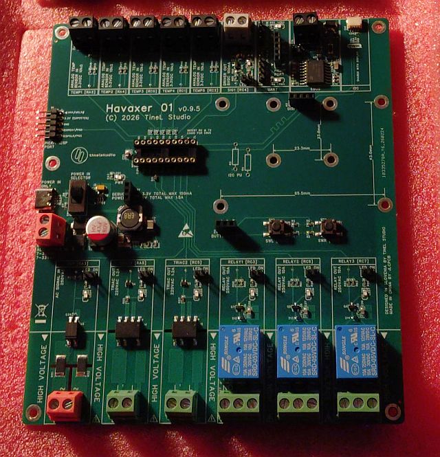
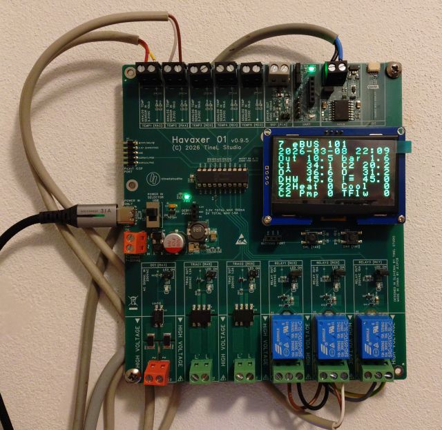
What changed since 0.9
This is where the board became the product it is now. Four of the five things wrong with 0.9 were fixed by replacing the part that caused them.
The power supply was rebuilt. The linear regulator went, replaced by a bridge rectifier and a switching buck converter. That is what made the alternative supply input accept AC as well as DC, either polarity, and a much wider voltage range - and it removed a part that reached 100 °C in normal use.
The on-board isolated eBUS adapter arrived. The 0.9 board had none; eBUS was an external third-party adapter hanging off the debug power header.
The signal driver output became a real driver. On 0.9 it was a resistor-limited 3.3 V output good for a few milliamps. From 0.9.5 it is a 5 V MOSFET output rated 100 mA, with a resettable fuse, a flyback diode and a TVS clamp.
The relays changed type, and gained PWM hold.
The triac snubbers were removed - see 0.9 below for why.
The inductors on the temperature inputs were removed - same.
The mains input resistors were upgraded from 350 V metal film to 500 V thick film parts.
Known problems
UART alone not working - issue #4open_in_new. Improved but not eliminated in 1.0.
Measurements 0.9.5
Same equipment as 1.0. Power over USB at 5.07 V.
The display figures are not comparable with 1.0. From 1.0 onwards the display test fills the whole screen; here it does not. The difference in the table below is the test, not the hardware.
Mains signal input
- Draw from the board's 5 V rail: 1.5 mA.
- At ~230 VAC the limiting resistors reach 33 °C (+13 K). Applied 237.1 VAC.
Mechanical relay output
- Coil current at 100 % PWM duty, cold: 73 mA.
- Coil resistance 68.5 Ω cold and 75.5 Ω warm.
- ~230 VAC at 11 A: the relay area reached 55 °C (+30 K). The relay component itself did not heat at all - the power traces underneath it did. This is the measurement that first showed where the heat comes from.
Relay coil PWM hold
| 100 % duty | 40 % duty | |
|---|---|---|
| Coil current, cold | 73 mA | 10 mA |
| Drop across the coil | 4.92 V | 1554 mV |
| Drop across the MOSFET | 112 mV | 3498 mV |
Solid state relay output
- Drive current per triac: 8 mA.
- Drive chain at 5.07 V in: 1138 mV across the triac IC, 3888 mV across the series resistor, 52 mV across the driving transistor.
- ~230 VAC at 1.34 A: 69 °C (+49 K).
Signal driver output
- Shorted: about 170 mA initially, settling near 125 mA as the fuse heats. From cold, measured at the supply: 145 mA.
- The fuse reached 65 °C (+45 K).
eBUS adapter
Measured from the board's 3.3 V side.
| Condition | Measured | Designed |
|---|---|---|
| Activated, bus disconnected | 10.5 mA | ≤ 18 mA |
| Activated, connected to a live bus | 8.5 mA | ≤ 18 mA |
| Activated, disconnected, receive shorted | 63.5 mA | ≤ 60 mA |
| Deactivated, receive pulled up | 42.5 mA | 0 |
| Deactivated, transmit pulled up | 64.5 mA | 0 |
| Activated, connected, transmit pulled up | 79.5 mA | ≤ 18 mA |
Pulling transmit up to 3.3 V heated the adapter to 175 °C and pulled 377 mA from the bus - the same as on 1.0, reached from the opposite direction, because the transmit polarity changed between the two revisions.
I2C display port
Display current at 3.3 V supply. Screen not filled - see the warning above.
| 0.96" HS96L03W2C03 | 0.96" APKLVSR JMD0.96D | 2.42" Hailege | |
|---|---|---|---|
| Display off | 0 mA | 0 mA | 0 mA |
| Contrast I | 2.5 mA | 3 mA | 23 mA |
| Contrast II | 3.5 mA | 4 mA | 28.5 mA |
| Contrast III | 5 mA | 6.5 mA | 41 mA |
Alternative power supply input
This is the circuit that 1.0 changed, so the numbers below are worth reading against the 1.0 table above.
| Input | Load | Bridge rectifier | Buck | 5 V out |
|---|---|---|---|---|
| 6.77 VDC | 330 mA | 61 °C (+41 K) | no rise | 5.00 V |
| 6.64 VDC | 600 mA | 88 °C (+68 K) | no rise | 4.84 V |
| 13.12 VDC | 245 mA | 34 °C (+14 K) | no rise | 5.07 V |
| 15.38 VDC | 330 mA | 39 °C (+19 K) | 5.06 V | |
| 15.21 VDC | 780 mA | 55 °C (+25 K) | 5.05 V | |
| 33.28 VDC | 245 mA | 25 °C (+5 K) | 28 °C (+8 K) | |
| 32.2 VDC | 780 mA | 35 °C (+15 K) | 38 °C (+18 K) |
The single bridge chip is the limit at the bottom of the input range, and at 6.64 V with a 600 mA load it both overheats and lets the rail sag. Replacing it with four discrete schottky diodes in 1.0 is what fixed that.
Power consumption
| Cold start | 266 mA |
| After a few minutes | 255 mA |
| Power | ≈ 1.5 W |
Sum of the individual lines: 288 mA. Do not read the difference against 1.0 as a regression - most of it is the display test change noted above.
Version 0.9
First prototype. Never sold, and never intended to be. It is on this page because the trajectory is the point: everything below was found by measuring, and every one of these is gone from the board you can buy.
| Design finished | 2025-12-21 |
| Put into production | 2025-12-21 |
| Inspecting | 2026-01-06 |
This revision was not safe to run at its own stated input range. None were sold and none should be used. It is documented, not supported.
What was wrong
A capacitor rated for 16 V sat on a rail that could reach 37 V. Applying 33 V destroyed it instantly - tested, and it did exactly that. Fixed by redesigning the supply in 0.9.5.
The temperature inputs had inductors that shorted the sensors to ground. They were removed on the prototypes by hand and designed out in 0.9.5.
The triac snubbers leaked enough current to run a light load with the triac switched off. A 3 W motor kept turning; a 60 W incandescent bulb behaved correctly. Removing the snubbers fixed it, and there has been no snubber on the triac outputs since.
The linear regulator overheated. At 15.45 V in and 299 mA out it reached 100 °C, 85 K above ambient - and 299 mA is not a large load for this board. It is what forced the switch to a buck converter in 0.9.5, and with it the ability to run from AC.
Measurements 0.9
Power over USB at 5.06 V. There is no eBUS section because the 0.9 board had no eBUS adapter.
Mains signal input
- At ~230 VAC the limiting resistors reach 32 °C (+16 K). Applied 230.5 VAC. The parts were 100 kΩ metal film rated 350 V, replaced in 0.9.5 by 500 V thick film.
- Voltage across the optocoupler input: 1.117 VAC, against 1.1 V typical.
Mechanical relay output
- Coil current: 48 mA. A different relay type from 0.9.5 onwards, and there was no PWM hold yet.
- ~230 VAC at a little over 10 A: the relay area reached 45 °C (+30 K), mostly from the power traces below it.
Solid state relay output
- Drive current per triac: 7.5 mA.
- 230 VAC at 1.35 A, with the snubber physically removed: 50 °C (+35 K).
Signal driver output
- Shorted: 3.5 mA. On this revision the output was a resistor-limited 3.3 V signal, not the 5 V driver it became in 0.9.5, so the figure is not comparable with anything later.
I2C display port
Display current at 3.3 V supply. Screen not filled.
| 0.96" HS96L03W2C03 | 0.96" APKLVSR JMD0.96D | 2.42" Hailege | |
|---|---|---|---|
| Display off | 0 mA | 0 mA | 0 mA |
| Contrast I | 3 mA | 3 mA | 30 mA |
| Contrast II | 3.5 mA | 4.5 mA | 35 mA |
| Contrast III | 5 mA | 7 mA | 47.5 mA |
Alternative power supply input
A linear regulator, 7-37 VDC in, 500 mA rated - DC only.
| Input | Load | Regulator |
|---|---|---|
| 13.08 VDC | 208 mA | 66 °C (+51 K) |
| 13.08 VDC | 299 mA | 89 °C (+74 K) |
| 15.45 VDC | 208 mA | 81 °C (+66 K) |
| 15.45 VDC | 299 mA | 100 °C (+85 K) |
More load than that was not attempted.
Power consumption
| Maximum observed | 208 mA |
| Power | ≈ 1 W |